Monday, June 24, 2024
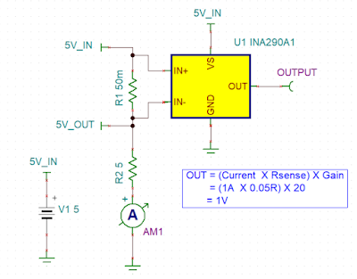
Ultra-Precise, Current-Sense Amplifier
Thursday, June 20, 2024
Driving a Bicolor LED from a Single Output Pin
This circuit showcases the control of a bi-colour LED from a single output pin using two PNP transistors. You can access the Java Script simulation link here:
👉 https://tinyurl.com/22y3w9er
The circuit comprises two NPN transistors for switching, one bi-colour LED, two resistors for base current control, another two resistors for collector current setting for each transistor, and two voltage sources. The first voltage source at the top outputs 24V to drive the LEDs, while the second voltage source supplies 3.3V at the base of the transistors to simulate logic control output from microcontrollers.
In the OFF position of the switch, both transistors are in the OFF state, and the LED on the right side is ON via a 10k resistor with an LED driving current of 2.2mA. When the switch is ON, both transistors are in the ON state, driving the LED on the left side, while the other LED is switched off because the transistor on the right side is on, pulling down the LED anode voltage.
Monday, June 17, 2024
Monday, June 10, 2024
Over Current Protection at Output Stage/ Pins
The purpose of this circuit is to restrict the output current to less than 20mA, and this limit can be adjusted using resistors R1 and R8. Furthermore, the circuit also can disconnect the input/output when the output short circuits to a high positive or negative voltage by limiting the current.
Additionally, the diode D1, located at the output and the 5V0 pin, serves to suppress the kick-back voltage from an inductive load. This occurs when the drivers are deactivated (stop sinking) and the stored energy in the coils causes a reverse current to flow into the coil supply through the kick-back diode.
How to use MOSFET for Hide Side Switching
I've crafted a circuit designed for high-voltage (up to 100V) and high-current (up to 33.6A) applications, specifically for switching loads on the high side. The carefully selected P-Channel MOSFET, Q1, boasts low ON resistance. To safeguard against exceeding the maximum gate-source voltage (VGS), I've incorporated R1 and R2. Another option involves including a Zener diode across the Gate and Source. In addition, a small signal N-Channel MOSFET, Q2, effectively controls the ON/OFF switching of the N-Channel MOSFET. When the ON/OFF control is low, Q2 remains OFF. Conversely, when it's high, Q2 activates, thereby reducing the P-Channel gate voltage via R2 and effectively limiting the current.
Friday, June 7, 2024
Overvoltage Protection
Hot-Swap Circuits with Inrush Current Limiter
To provide continuous current sensing and limiting, this hot-swap circuit uses a PNP transistor and a current sense resistor of 0.333R. Wh...

-
This EMI filter includes a common-mode filter and a differential-mode filter. Generally Differential mode filter filters noise less than 3...
-
I've crafted a circuit designed for high-voltage (up to 100V) and high-current (up to 33.6A) applications, specifically for switching ...


