As a picture speaks a thousand words, adding an image object to the schematics is very handy for design review. Prefer method of adding PNG file as below.
Showing posts with label Altium Designer. Show all posts
Tuesday, May 17, 2022
Tuesday, May 10, 2022
Altium Designer : PCB Planes Pullback implementation
There are many ways to implement polygon planes pullback in Altium. One of my prefer way is utilizing design rules as below.
Alternatively, we can make use of keep-out layer to define polygon pullback.
Thursday, May 5, 2022
Altium Designer : Solving the Component Management Challenge with Alticve BOM
ActiveBOM is a powerful Bill of Materials management editor that brings comprehensive BOM management tools together with Altium's powerful part-information aggregation technologies, helping you manage the component selection challenge.
Friday, May 3, 2019
Tuesday, January 8, 2019
Altium Designer : Defining Solder Mask Expansion/ Relief
Altium default value is 4 mil and solder mask expansion can be defined according to PCB manufacturer capability.
Monday, December 10, 2018
Friday, December 7, 2018
Thursday, December 6, 2018
Wednesday, December 5, 2018
Tuesday, December 4, 2018
Monday, December 3, 2018
Altium Designer : Creating Custom Board Outline and Keepout Area
It is a good design practice to add keepout area along the board outline. Recommended keep out line thickness is 20 mil.
Friday, November 23, 2018
Altium Designer: Useful Shortcuts for Component Placement
- Rotate counterclockwise by 90 degrees while moving an object : SPACEBAR
- Align selected objects by top edges : SHIFT + CTRL + T
- Distribute selected objects equally in horizontal plane : SHIFT + CTRL + H
- Align selected objects by left edges : SHIFT + CTRL + L
- Align selected objects by right edges : SHIFT + CTRL + R
- Distribute selected objects equally in vertical plane : SHIFT + CTRL + V
- Align selected objects to grid : SHIFT + CTRL + D
- Align selected objects by bottom edges : SHIFT + CTRL + B
Thursday, November 22, 2018
Altium Designer : Pcb Panelization
On the Place tab, Select Embedded Board Array/ Panelize. Click anywhere in the PCB area. Under Properties menu, select your PCB and set desired Column margin and Row spacing.
Altium Designer : Creating Board Outline From Mechanical Outline and Making Cutout Holes
Select Mechanical Outline. Under Properties menu, Change Mechanical outline layer to user defined board outline layer.
To create custom board shape, select board outline that has been created. On the Design Tab, in the board shape, select Define from selected Objects.
To create a cutout hole, select the desired outline. On the Tool Tab, in the Convert, select Create Boardcutout from selected primitives.
Altium Designer, Shortcuts for Viewing, Changing Grid and Snap Setting
Toggle measurement Unit : Q
Accessing Grid menu : G
Changing snap setting : SHIFT + E
Switching 2D and 3 D View : 2 & 3
Fit all objects into view : CTRL + PAGE DOWN
Zoom in around cursor (zooms around cursor, position the cursor first) : CTRL + Mouse-wheel up (or PAGE UP)
Zoom out : CTRL + Mouse-wheel down (or PAGE DOWN)
Subscribe to:
Posts (Atom)
Ultra-Precise, Current-Sense Amplifier
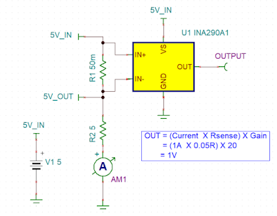
This ultra-precise current sense amplifier that can measure voltage drops across shunt resistor, R1 over a wide common mode range from 2....
-
Voltage divider resistor network is used to step monitored voltage down to the range as necessary for A/D conversion. Passive low-pass f...
-
Select Mechanical Outline. Under Properties menu, Change Mechanical outline layer to user defined board outline layer. ...