Tuesday, September 1, 2020

Electronic Load Fundamentals


What is an electronic load?

An electronic load is a test instrument designed to sink current and absorb power out of a power source. If a power supply is used to power a device, an electronic load is used to test the power supply by emulating the device under test (DUT).


An electronic load is a programmable instrument that offers the user various modes of control such as constant voltage (CV), constant current (CC), constant power (CP) or constant resistance (CR).

Who uses electronic loads?

Device manufacturers and design engineers use electronic loads to test numerous power devices such as power supplies, DC-DC converters, chargers, adapters, batteries, solar panels, fuel-cells, and more.

Why do engineers use electronic loads instead of a fixed value power resistor?

In situations where you need a purely resistive load and no closed loop control is required, it is sufficient to use a fixed value power resistor. A fixed value resistor presents many limitations. It is not adequate for loading and testing power sources that have complex testing requirements. Such tasks require sophisticated electronic load features to validate the various states of operation.

Constant current operation mode

Constant current (CC) is the most frequent mode in which an electronic load is used. In constant current mode, the load will sink the programmed current independently from the output voltage which is typically forced by the voltage source connected to it (for example a battery).

Constant voltage operation mode

In constant voltage (CV) mode the electronic load sets a fixed programmable voltage across its terminals independently from the input current. In CV mode, the current is set by the current source connected to it – for example, a current charging circuit or a LED current driver. The load adjusts its resistance dynamically to attain the programmed voltage at any current established by the current source under test.

Constant resistance operation

In constant resistance (CR) mode, the load acts as a fixed programmable power resistor. An electronic load’s CR mode is well-suited for loading a power source that is either a voltage or current source. When the load connects to a voltage source it sinks a current equal to the source potential divided by the programmed resistance value.


Friday, July 17, 2020

Low cost temperature sensor


Low cost temperature sensor can be achieved by using diode or transistor (by shorting Base and Collector). When constant current passes through the base-emitter junction it produces a voltage between the base and emitter (Vbe) that is a linear function of the absolute temperature. 
The overall forward voltage drop has a temperature coefficient of approximately 2 mV/°C. The semiconductor junction sensor’s voltage versus temperature is much more linear than that of a thermocouple or resistive temperature device (RTD). 

Friday, April 24, 2020

How to ruggedized Arduino Boards

As we all know that Arduino boards are low cost and are not designed to be used in a harsh environment. However, we can ruggedize these boards by adding proper protection circuitry so that it can be used for industrial environments.

One company in the States is designing ruggedized Arduino-compatible microcontroller boards and they posted on their website interesting ways to destroy the boards as well as the fix. Here is the link.


Implementing Ship Mode to Your Product

As the presence of global manufacturing and distribution increases, many original equipment manufacturers are looking for creative ways to extend battery life during shipping and shelf life at big-box warehouses. Keeping the battery sufficiently charged during shipment enables a consistent out-of-box experience for the end-user. A solution that has gained popularity is the use of a ship mode feature that keeps devices in a low-power state during shipment and while on the shelf. Here is my solution using a load switch from TI, TPS22915B.
This is how the circuit works. Before the button is pressed, the solution is in ship mode, meaning that the system is not powered and theTPS22915B load switch is turned off. When the button is pressed, the voltage from the battery is passed through the PMOS to the ON pin of the TPS22915B. The voltage enables the TPS22915B, brings VOUT high, turns off the PMOS, and powers the system. The ON pin is pulled up to VOUT, which keeps the load switch enabled even after the button is released.

Wednesday, April 1, 2020

Making your own PCB by Etching method

1) Artwork Printing: 

Print your artwork on a transparent sheet.

2) Exposing:

Kinsten Presensitized PCB is using for this prototype as it is low cost and easy to work. Remove light-proof protective film and expose the board in the Kinsten UV exposure box for 90 seconds.
Align the artwork with the PCB inside the vacuum clamp, leave it inside the exposure box for about 5 minutes.

3) Developing:

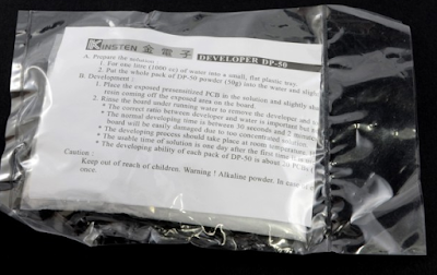
A sachet of DP-50 developer is mixed with 1 liter of 25°C water in a plastic container. The exposed PCB is gently agitated in solution. The exposed areas of resist will dissolve into the solution, leaving the green resist in areas that were not exposed to UV light as below.

4) Etching:

Etching copper is done in the Kinsten Etching Tank for 4 to 10 minutes. Pour enough etching solution (Ferric Chloride or Ammonium Persulphate) into the tank and immerse the board. Use the air pump to allow the etchant to be bubble agitated until the unwanted copper foil etched away, only the circuit patterns left. Rinse the board with plenty of water.
Remember “Safety First” always wear rubber gloves and protective eyewear when working with this etching compound. Kindly take note, once you've etched your board, the leftover solution should not pour it down the drain (legally). Take it to a hazardous waste facility.

Here is the final outcome. To get better results, make PCB trace thickness at least 10 or 12 mil and leave the wider gap between trace and GND copper pour.


Friday, March 20, 2020

Estimating Product life Span

In order to predict the lifetime of a product, manufacturers usually conduct accelerated temperature & Humidity test. We usually conduct the accelerated test under the conditions that are much more severe than the actual operating conditions and record test hours, time-to-failure. Then we estimate/ calculate the product life-span using Peck's Power Law.

In the below example, the estimated lifetime of the product under test is 12 months if it survives for 96 hours at 80 °C with 90% RH. Assuming the product normal upper operating limit of 40 °C and 50% RH, we have got acceleration factor 92.48.


Digital filtering technique , ADC Filter


A digital filter system usually consists of an analog-to-digital converter (ADC) to sample the input signal, followed by a microprocessor and some peripheral components such as memory to store data and filter coefficients etc.
Program Instructions (software) running on the microprocessor implement the digital filter by performing the necessary mathematical operations on the numbers received from the ADC.

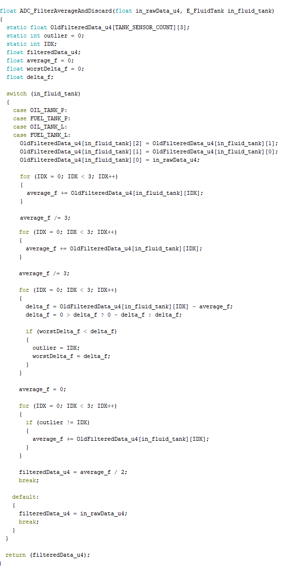
Here is a simple digital filter which identifies and reject transient response signal. It basically returns average of best two samples of the last three. The third sample is discarded.

Algorithm:
1. Calculate the average of the last 3 samples
2. Identity the sample furthest from the mean value (which is the outlier)
3. Discard the outlier and average the remaining two samples
4. Returns float value of the averaged data (y(i)).


Ultra-Precise, Current-Sense Amplifier

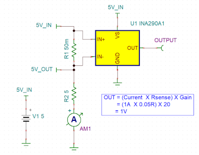
   This ultra-precise current sense amplifier that can measure voltage drops across shunt resistor, R1 over a wide common mode range from 2....