Friday, March 20, 2020

Estimating Product life Span

In order to predict the lifetime of a product, manufacturers usually conduct accelerated temperature & Humidity test. We usually conduct the accelerated test under the conditions that are much more severe than the actual operating conditions and record test hours, time-to-failure. Then we estimate/ calculate the product life-span using Peck's Power Law.

In the below example, the estimated lifetime of the product under test is 12 months if it survives for 96 hours at 80 °C with 90% RH. Assuming the product normal upper operating limit of 40 °C and 50% RH, we have got acceleration factor 92.48.


Digital filtering technique , ADC Filter


A digital filter system usually consists of an analog-to-digital converter (ADC) to sample the input signal, followed by a microprocessor and some peripheral components such as memory to store data and filter coefficients etc.
Program Instructions (software) running on the microprocessor implement the digital filter by performing the necessary mathematical operations on the numbers received from the ADC.

Here is a simple digital filter which identifies and reject transient response signal. It basically returns average of best two samples of the last three. The third sample is discarded.

Algorithm:
1. Calculate the average of the last 3 samples
2. Identity the sample furthest from the mean value (which is the outlier)
3. Discard the outlier and average the remaining two samples
4. Returns float value of the averaged data (y(i)).


Friday, February 21, 2020

Friday, August 2, 2019

Reference Book and PCB Design Guidelines


Book Link is Here..

This is an old book but still useful and good techniques to reduce noise in electronic systems.


This is one of the best guidelines I have come across.

Thursday, May 30, 2019

Clearance Holes for Metric Fasteners

When we do PCB board design, it is good to know how much clearance we need for screw holes. General Screw size and clearances for holes can be seen in the table below.

PCB Design : Via Current Carrying Capacity

Maximum via current carrying capacity can be calculated using Saturn PCB Design Toolkit
Commonly used via size and current carrying capacity are as below.


Wednesday, January 9, 2019

Absolutely free and easy to use Software Tool for Engineers

1) gerbv - A Free/Open Source Gerber Viewer


You can download the source code from this page.

2) View 3D objects with STP viewer

Direct download link is here.

3) FreeCAD

Download Link is here.

DepanelingTab Routing

Board assemblies can be de-tabbed using perforated breakaway tabs, v-grooves break away tabs, or hand-cutting with a de-tabbing tool. For Tab and V-Score (i.e. PCB's that must be sheared along an edge):
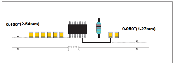
1. Traces and vias should be a minimum of 0.050"(1.27 mm) away from routed/scored edge.
2. Components should be a minimum of 0.100"(2.54 mm) away from routed/scored edge.
These rules are to help prevent components or board damage during the depaneling process and prevent flooding during the wave soldering process.


For 0.062" (1.6 mm thickness) Printed Circuit Boards:

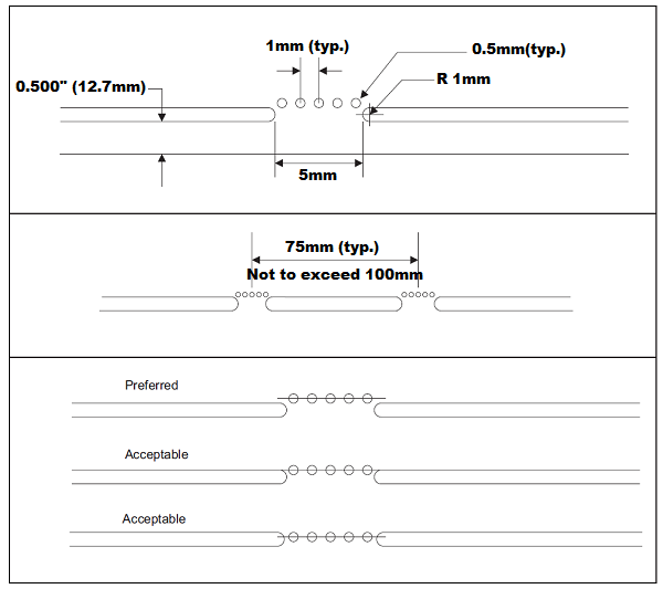
1. Perforation holes should be typically spaced at 1 mm intervals.
2. Tab routed with 1 mm radius.
3. Routed slot should be 2 mm minimum, for single image panels. Use 3 mm routed slots when two or more boards are in a panel. This allows for more accurate edge dimensions.
4. 75 mm typical distance between tabs, not to exceed 100 mm.
5. Place tabs approximately 25 mm from corners to reduce sagging during reflow or wave soldering.
6. Desirable to have at least one tab per side.
7. Slight inset of perforation is preferred; it provides an edge which requires little or no additional labor to clean up.

NOTE: Two parallel edges are required for a PCB to be processed in the SMT line. This is to prevent skewing through the conveyor system. All odd shaped PCB's MUST have edge rails incorporated to meet this requirement. Custom reflow fixtures will be made if this requirement is not met.


Tuesday, January 8, 2019

SMD and NSMD Pad Configurations

Two types of PCB solder mask openings commonly used for surface mount leadless style packages are:

1. Non Solder Masked Defined (NSMD)
2. Solder Masked Defined (SMD)

As their titles describe, the NSMD contact pads have the solder mask pulled away from the solderable metallization, while the SMD pads have the solder mask over the edge of the metallization, as shown above. With the SMD Pads, the solder mask restricts the flow of solder paste on the top of the metallization which prevents the solder from flowing along the side of the metal pad. This is different from the NSMD configuration where the solder will flow around both the top and the sides of the metallization.

Typically, the NSMD pads are preferred over the SMD configuration since defining the location and size of the copper pad is easier to control than the solder mask. This is based on the fact that the copper etching process is capable of a tighter tolerance than the solder masking process. This also allows for visual inspection of solder fillet.

In addition, the SMD pads will inherently create a stress concentration point where the solder wets to the pad on top of the lead. This stress concentration point is reduced when the solder is allowed to flow down the sides of the leads in the NSMD configuration.

Cool Electronic Circuit Simulator

This online circuit simulator is easy to use and useful for simple circuit simulations.


Ultra-Precise, Current-Sense Amplifier

   This ultra-precise current sense amplifier that can measure voltage drops across shunt resistor, R1 over a wide common mode range from 2....